Series: The Evolution of Surface Mount Technology
Welcome to Part 1 of our comprehensive 10-part series charting the history of electronics manufacturing. Before we explore the microscopic world of 008004 components, we must understand the giants that came before.
- The Pre-Dawn of SMT: The Era of Through-Hole
- The Birth of Flat Packs (1960s-1970s)
- The Consumer Revolution (1980s)
- The War on Size (Passive Components)
- The Package Wars (Active Components)
- The Process Evolution I – Placement
- The Process Evolution II – Soldering
- The Area Array Revolution (1990s-2000s)
- The Green Shift & High Reliability
- Industry 4.0 and Beyond
The Pre-Dawn of SMT: The Era of Through-Hole and the Necessity of Change
Before the sleek, pocket-sized smartphones of today could exist, the electronics industry was dominated by a manufacturing method that was robust, reliable, and unmistakably heavy: Through-Hole Technology (THT). To truly appreciate the revolutionary nature of Surface Mount Technology (SMT), we must first step back into the mid-20th century to understand the “Big Iron” world it replaced.
The Tyranny of the Drill: Inside the THT Process
From the transistor radio boom of the 1950s through the rise of personal computing in the 1970s, the Printed Circuit Board (PCB) assembly process was defined by one mechanical action: drilling.
In this era, every single electronic component—whether a simple carbon resistor, a ceramic capacitor, or a complex Dual In-line Package (DIP) integrated circuit—was manufactured with long, sturdy metal leads. The assembly process was physically demanding and mechanically complex:
- Drilling: Manufacturers had to drill holes through the fiberglass PCB substrate for every single pin. For a complex board, this meant thousands of precision holes.
- Insertion: The component leads were inserted through these holes from the top side of the board.
- Clinching: On the bottom side, the leads were bent (clinched) to hold the component in place mechanically before soldering.
- Wave Soldering: The board was passed over a “wave” of molten solder, which wicked up the holes to form a joint.
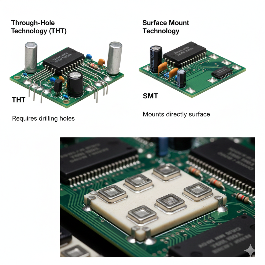
This method had distinct advantages that keep it alive even today for high-power electronics and heavy-duty machinery. The mechanical strength provided by the leads passing through the board offered immense durability against physical stress and vibration. Furthermore, it was forgiving; engineers could easily prototype and repair these boards by hand using simple soldering irons.
However, as the world moved from analog radios to digital computing, the physical limitations of THT began to stifle innovation.
The Three Barriers to Progress
By the late 1960s, engineers at pioneering companies like IBM, Philips, and Texas Instruments began to hit a “brick wall.” They identified three critical limitations of Through-Hole Technology that threatened to halt the advancement of computing power:
1. The Real Estate Problem (Density)
Drilling holes requires physical space. You simply cannot drill holes too close together without cracking the fiberglass substrate. More importantly, a hole is a “via” that goes all the way through the board, effectively blocking that specific coordinate on all layers of the PCB.
In the THT era, double-sided assembly was nearly impossible. Because the leads from the top components protruded through the bottom, there was no room to place components on the underside. This effectively wasted 50% of the board’s surface area, severely limiting how much computing power could be packed into a device.
2. The Physics Problem (Parasitics)
As engineers pushed circuit speeds higher, the components themselves became the problem. The long metal leads of DIP packages and axial resistors acted like tiny antennas.
In electrical engineering terms, these leads introduced parasitic inductance and capacitance. At low frequencies, this didn’t matter. But at high frequencies (the kind needed for faster computers), these “stray” electrical properties distorted signals, creating noise and cross-talk. To build faster computers, the leads had to go.
3. The Manufacturing Problem (Cost & Automation)
Drilling thousands of holes is expensive. Drill bits wear out, break, and require maintenance. Furthermore, while automatic insertion machines existed (like the iconic Universal Instruments axial inserters), they were massive, loud, and limited in speed.
A typical high-speed placement machine today can place 100,000 components per hour. In the THT era, inserting 5,000 components per hour was considered a marvel of engineering. The industry needed a way to place components faster than they could be mechanically inserted.
The Proto-SMT: Hybrid Circuits & The Cold War
Interestingly, the seeds of SMT were not sown in consumer electronics, but in the high-stakes world of the Cold War. The military and aerospace sectors desperately needed to reduce the weight of guidance systems in missiles and aircraft. Every gram saved on electronics meant more range or payload.
In the 1960s, “Hybrid Microcircuits” began to appear. These were the true ancestors of SMT. Instead of standard green fiberglass (FR4) boards, hybrids used ceramic substrates.
- Printed Components: Engineers figured out they could screen-print resistors directly onto the ceramic surface using conductive, resistive inks—no leads required.
- Leadless Bonding: Transistors and capacitors were bonded directly to the surface using conductive epoxy or wire bonding.
This proved that electronic circuits didn’t need holes to function. They could be built on the surface.
IBM’s Solid Logic Technology (SLT): The Turning Point
Perhaps the most significant commercial precursor to modern SMT was IBM’s Solid Logic Technology (SLT), introduced in 1964 for the legendary System/360 mainframe.
IBM realized that standard DIP packages were too bulky for the computing power they envisioned. They developed a revolutionary method of creating small ceramic squares (about the size of a fingernail) with metal contact pads on the surface rather than leads. They utilized a “flip-chip” method—placing glass-encapsulated transistors upside down onto the ceramic module and soldering them directly to the substrate using tiny copper balls.
While SLT was a modular system used to build the computer rather than a direct board assembly method, it proved a vital concept to the world: You can trust a solder joint to provide both the electrical connection and the mechanical support. You do not need a metal lead passing through a hole to hold a component in place.
The Stage is Set for a Revolution
By the end of the 1970s, the pressure was mounting on all fronts.
Japanese consumer electronics manufacturers like Sony and Panasonic were racing to make radios and cassette players small enough to fit in a pocket. American defense contractors needed lighter, faster electronics. The drill bit had reached its limit.
The industry was desperate for a new standard. They needed components that had no leads, required no holes, and could be placed automatically by machines at blinding speeds. The “Planar Mounting” revolution was about to begin, setting the stage for the explosive growth of the 1980s and the birth of the modern electronics era.
Stay tuned for Article 2: The Birth of Flat Packs (1960s-1970s).